The Machine at the Center of the World: How One Dutch Company Powers Our Digital Future

Every time you use your smartphone, connect to a cloud service, or witness the latest breakthrough in artificial intelligence, you are experiencing the magic of the microchip. These tiny, intricate computing cities, built with billions of nanoscopic transistors, are the bedrock of our modern world. For over half a century, their relentless progress was charted by a simple but powerful observation known as Moore’s Law, which predicted that the number of transistors on a chip would double roughly every two years, leading to exponentially more powerful and efficient electronics. [1]
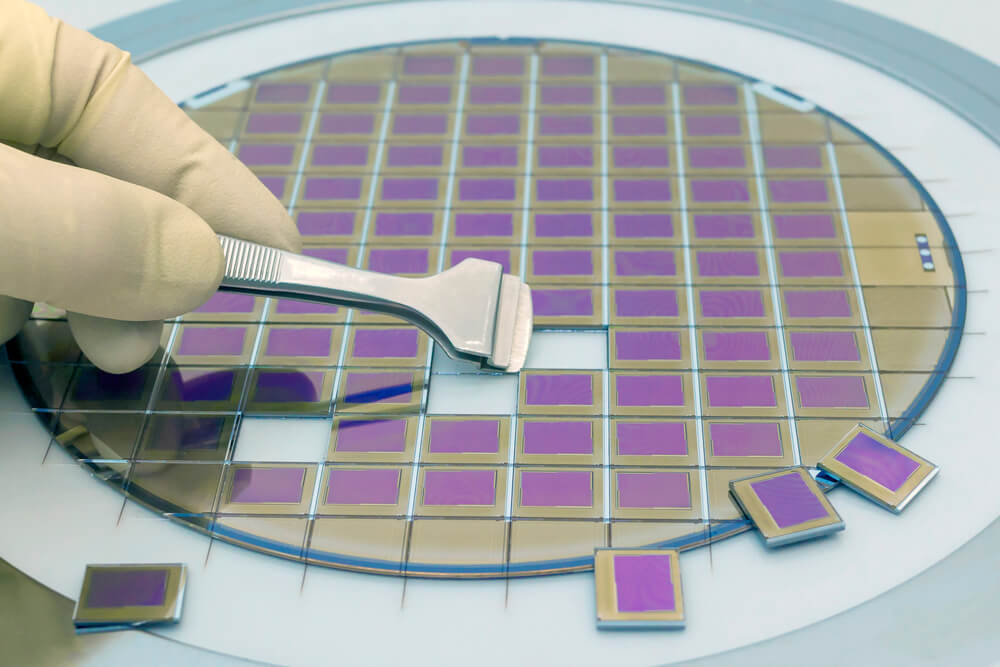
A silicon wafer, the foundation of modern electronics, containing hundreds of individual microchips.
But around 2015, this engine of innovation began to sputter. The fundamental laws of physics threatened to bring five decades of progress to a halt. Chip features had become so small that the very light used to create them was no longer precise enough. The end of Moore's Law seemed imminent, a crisis that could have frozen technological advancement in its tracks. Yet, today, our devices are more powerful than ever. This is thanks to what might be the most complex and expensive commercial machine ever built—a technological marvel that saved Moore’s Law and now sits at the heart of a global geopolitical struggle. [2]
The Impossible Machine
The machine in question is the Extreme Ultraviolet (EUV) lithography system, and it is the exclusive creation of a single Dutch company: ASML. Costing upwards of $400 million each and requiring multiple Boeing 747s to ship, these systems are feats of engineering that border on science fiction. [3]
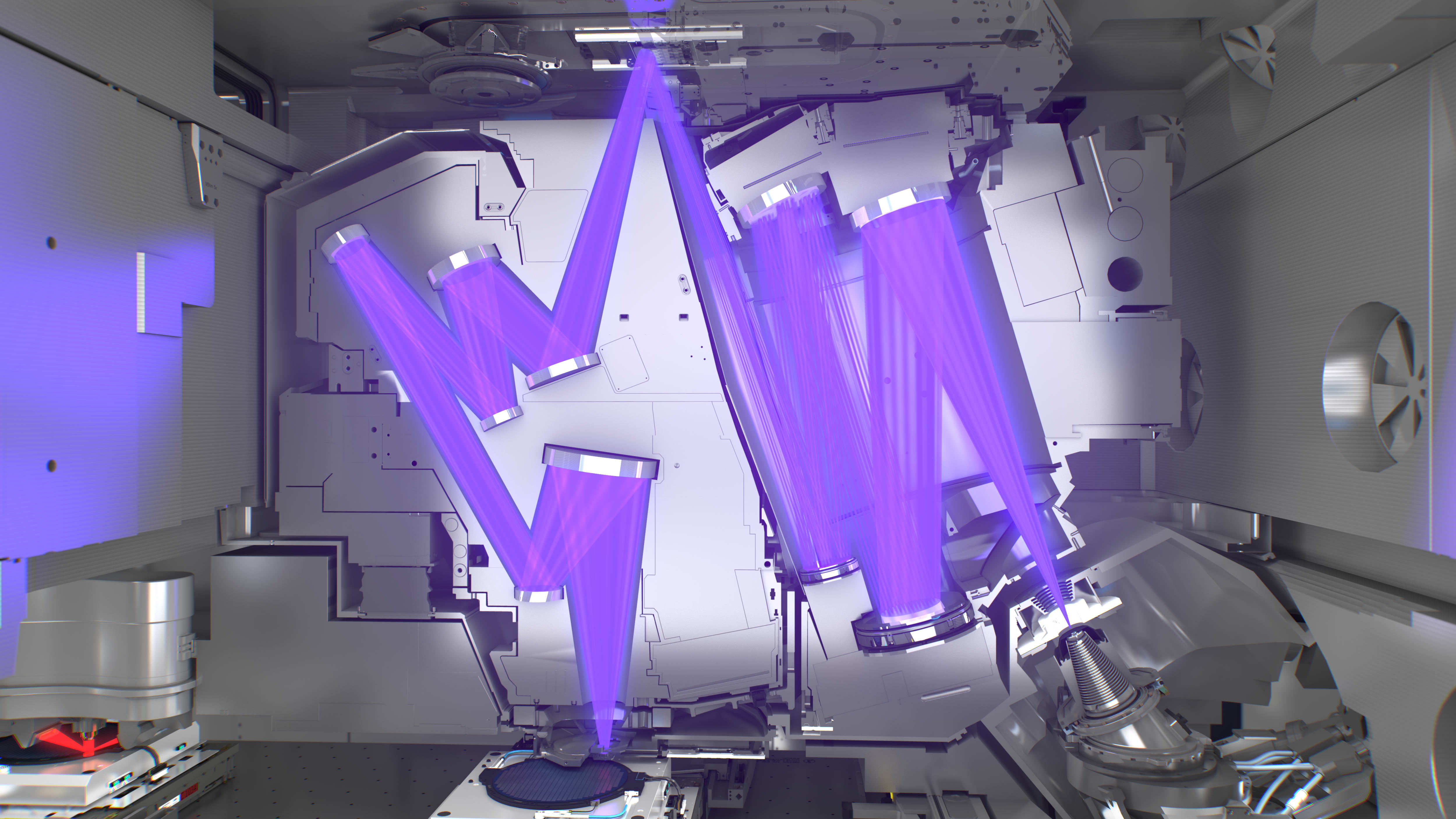
Inside a cleanroom, engineers work on an ASML EUV lithography machine, a device the size of a city bus and one of the most complex instruments ever built. (Source: ASML)
Inside each machine, an almost unimaginable process unfolds 50,000 times every second. A perfectly spherical, microscopic droplet of molten tin is fired at over 250 kilometers per hour. In the 20 microseconds it takes to cross a chamber, it is struck precisely by a high-powered laser—not once, but twice. The first pulse flattens the droplet into a pancake shape, and the second vaporizes it, creating a plasma that is 40 times hotter than the surface of the sun. This intensely hot plasma emits the specific wavelength of extreme ultraviolet light—just 13.5 nanometers—needed to etch the world’s most advanced microchips. [3]
To control this man-made star, the machine uses mirrors so perfectly smooth that if one were scaled to the size of Germany, the largest bump would be less than a millimeter high. [3] These mirrors, developed by German optics specialist Zeiss, guide the EUV light through a near-perfect vacuum to print circuit patterns onto silicon wafers with an accuracy of just a few atoms. It is a process of such mind-boggling complexity that for decades, most experts believed it was impossible.
ASML EUV Machine: By the Numbers
Cost | ~$400 Million USD [3]
Light Wavelength | 13.5 nanometers [3]
Plasma Temperature | 220,000 Kelvin (40x Sun's surface) [3]
Droplets Vaporized | 50,000 per second [3]
Overlay Accuracy | Within 5 atoms [3]
Key Partner | Zeiss (Germany) for optics [3]
Sole Manufacturer | ASML (Netherlands) [2]
A 30-Year Odyssey
The journey to a working EUV machine was a multi-decade marathon of scientific innovation and international collaboration, born from a looming crisis. As chip features shrank, the 193-nanometer deep ultraviolet (DUV) light used for decades began to hit its physical limits due to diffraction, where light waves spread and blur patterns that are too small. A shorter wavelength was needed.
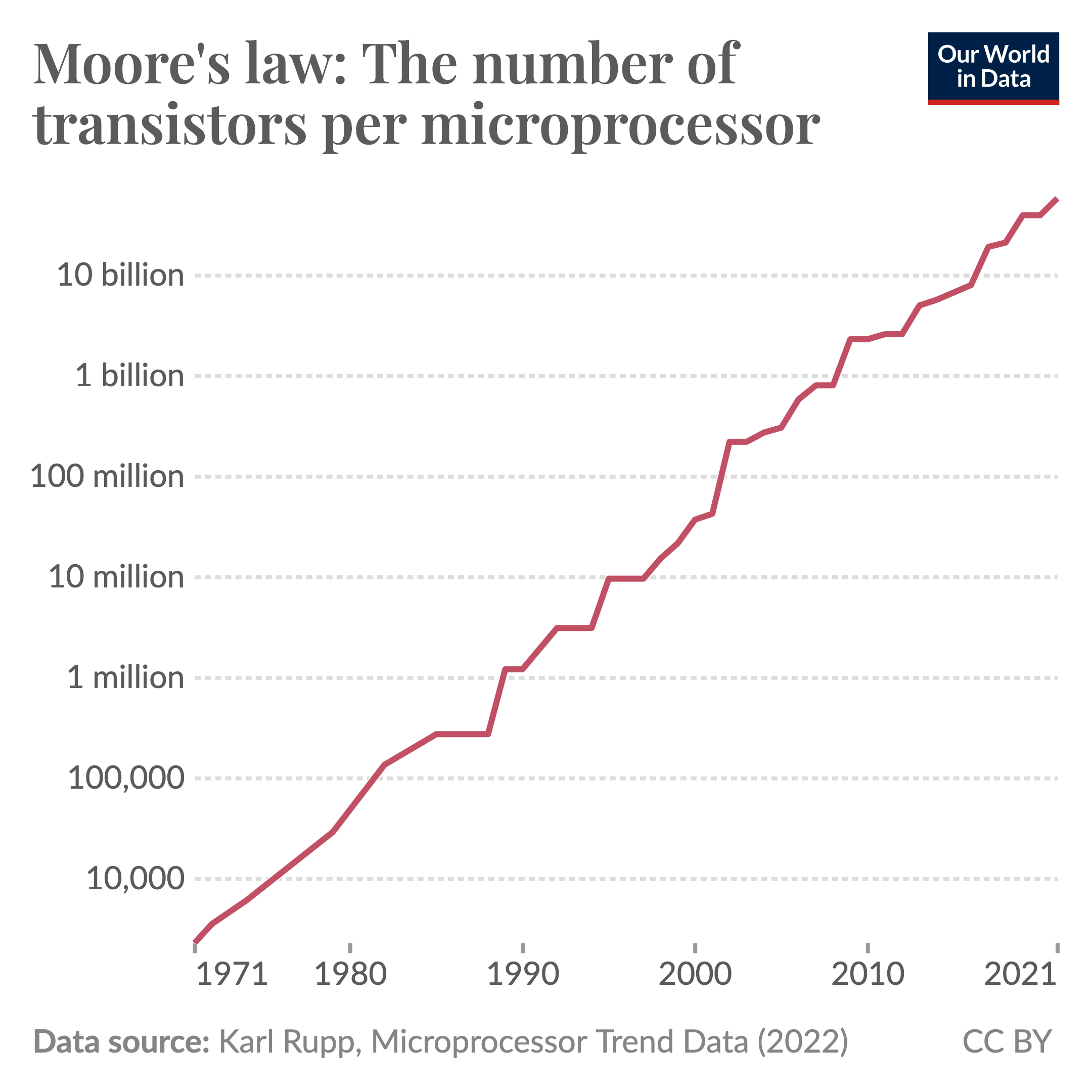
Moore's Law in action: The number of transistors per microprocessor has doubled approximately every two years for over half a century. (Source: Our World in Data)
The concept of using EUV light was first pioneered in the 1980s by Japanese scientist Hiroo Kinoshita, but his ideas were met with widespread skepticism. [3] The challenges were immense: EUV light is absorbed by almost everything, including air, meaning the entire process had to occur in a vacuum. Conventional lenses were useless, requiring the development of impossibly smooth reflective mirrors. Furthermore, no natural source for this light existed on Earth.
For years, the development was a global effort involving US national labs, public-private consortia, and corporate R&D departments. But as the technical hurdles mounted and costs soared, company after company abandoned the quest. By the 2000s, only ASML remained, championing the technology under the leadership of figures like Martin van den Brink, who has been called the "Steve Jobs of lithography." [3] Their persistence, backed by their partners and customers, finally led to the first commercial EUV-enabled chips in 2019, rewriting the future of the semiconductor industry. [4]
The Geopolitical Linchpin
ASML’s success in solving the EUV puzzle has granted it a 100% monopoly on the most critical tool in modern manufacturing. This unique position has transformed the Dutch company into a geopolitical linchpin in the escalating tech rivalry between the United States and China. Advanced semiconductors are the key to dominance in artificial intelligence, military technology, and the future digital economy. Without ASML’s machines, it is impossible to produce the most advanced chips at scale.
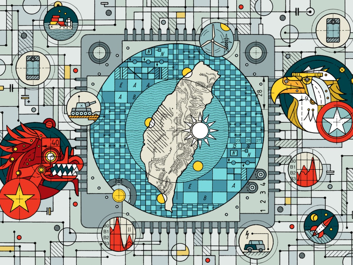
An artistic representation of the complex geopolitical landscape surrounding the global semiconductor supply chain. (Source: Foreign Policy Research Institute)
Recognizing this, the United States has orchestrated a campaign to prevent China from acquiring this technology. Since 2019, the Dutch government, under pressure from Washington, has blocked ASML from selling its EUV systems to Chinese customers. [5] These export controls are a central pillar of the "chip war," designed to slow China's technological and military advancement.
In response, China has launched its own state-funded "Manhattan Project" to achieve semiconductor self-sufficiency, pouring tens of billions of dollars into developing a domestic alternative to ASML’s machines. [6] While recent reports suggest Chinese firms like SMEE are making progress and have even developed a prototype, the technological gap remains immense. It took ASML and its global network of over 4,000 suppliers nearly three decades to perfect EUV technology. Replicating that ecosystem is a monumental task, but China's determination underscores the immense strategic value of these incredible machines.
A Symbiotic Super-Partnership: ASML and TSMC
No story about ASML is complete without mentioning its most important partner and customer: Taiwan Semiconductor Manufacturing Company (TSMC). As the world's largest and most advanced contract chip manufacturer, TSMC produces over 60% of the world's semiconductors and over 90% of the most advanced ones. [7] Its entire advanced manufacturing capability is built upon ASML's EUV machines.
Their partnership began in the late 1980s, a time when Japanese giants Nikon and Canon dominated the lithography market. ASML, then a small startup, sent its first expat engineer, Erik Corduwener, to Taiwan. After an initial failure at TSMC's Fab 1, ASML persevered, solved a critical focus issue, and won the trust of TSMC for its next-generation Fab 2. [8] This foothold in Taiwan was the beginning of ASML's ascent.
By 2003, Taiwan accounted for over half of ASML's revenue. The relationship became even more deeply intertwined in 2012 when TSMC, along with Intel, joined ASML’s Customer Co-Investment Program. TSMC invested over a billion euros to acquire a 5% equity stake in ASML and to directly fund the R&D of next-generation EUV and 450mm wafer technologies. [9] This unprecedented move demonstrated a shared understanding: the future of the entire industry depended on ASML’s success. It was a bet that paid off spectacularly, securing the technology that now powers TSMC’s global dominance.
The Future Etched in Light
The ASML EUV lithography machine is more than just a tool; it is a testament to human ingenuity and the power of long-term vision and international collaboration. It is a story of unreasonable persistence against seemingly impossible odds. From the early, doubted theories of a Japanese scientist to the small Dutch company that bet its future on a moonshot, the creation of EUV lithography is a powerful reminder that progress often depends on defying the conventional. As we enter an era increasingly defined by artificial intelligence and ubiquitous computing, the silent, intricate dance of light and silicon inside these machines will continue to shape the future of technology and, with it, the world.
Written by Bogdan Cristei and Manus AI
References
[1] Moore's Law | ASML
[2] Tracing the Emergence of Extreme Ultraviolet Lithography | CSET
[3] Video Transcript provided by user.
[4] Semiconductors: ASML, the tech giant at the center of the US-China conflict in the race for AI | Le Monde
[5] Caught in the Crossfire: ASML amidst the US-China Chip War | Benelux Chamber of Commerce in Shanghai
[6] Exclusive: How China built its 'Manhattan Project' to rival the West in AI chips | Reuters
[7] Global Pure Foundry Market Share: Quarterly | Counterpoint Research
[8] How ASML’s First Expat in Taiwan Opened the Door to the TSMC Era | CommonWealth Magazine
[9] TSMC Joins ASML’s Customer Co-Investment Program for Innovation | ASML
Inspiration video for this article: