The Unrelenting Rise of Silicon Photonics: A Technological Odyssey
From Heretical Idea to AI Revolution—The Complete Story of Light on Silicon
Written by Bogdan Cristei and Manus AI
Prologue: The Impossible Dream
In 1985, when Richard A. Soref published his seminal paper proposing that silicon—the workhorse of electronics—could also be used for photonics, the idea was considered heretical [1]. Silicon doesn't emit light efficiently. It doesn't modulate light well. It seemed fundamentally unsuited for the task. Yet Soref saw something others didn't: the potential to leverage the world's most advanced manufacturing infrastructure—CMOS fabrication—to build optical circuits at unprecedented scale and cost.
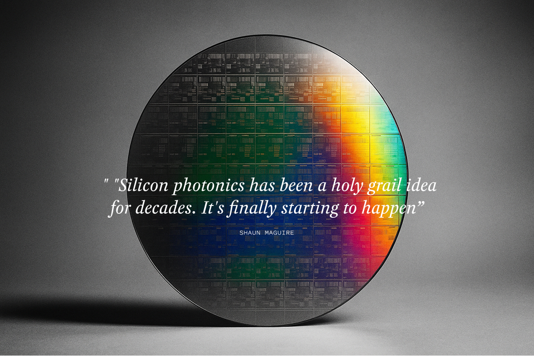
Four decades later, silicon photonics is no longer a curiosity. It powers the data centers that run our AI models, connects chips in supercomputers, and promises to revolutionize computing itself. In October 2025, Sequoia Capital—one of the world's most prestigious venture capital firms—declared: "Silicon photonics has been a holy grail idea for decades. It's finally starting to happen... I think the impact of silicon photonics in the next 50 years will be similar to the impact of silicon electronics in the last 50." [2]
This is the story of how we got here—a technological odyssey spanning from the 1980s to today, driven by brilliant researchers who refused to accept "impossible" as an answer.
Part I: The Foundation (1980s-1990s)
Richard Soref: The Founding Father
The field of silicon photonics traces its origins to a single insight by Richard A. Soref, then a researcher at the Air Force Research Laboratory. In 1985, Soref was working on fiber-optic communications when he realized that silicon's electronic properties could be exploited for optical applications [3].
His breakthrough came from understanding the free-carrier plasma dispersion effect—a phenomenon where changing the concentration of free electrons and holes in silicon changes its refractive index. This meant you could modulate light by applying an electric field, just as you control current in a transistor. In 1987, Soref and Brian Bennett published their landmark paper "Electrooptical effects in silicon" in the IEEE Journal of Quantum Electronics [4], laying the theoretical foundation for silicon modulators and switches.
But theory was one thing. Making it work was another.
The Silicon-on-Insulator (SOI) Revolution
The key enabling technology was silicon-on-insulator (SOI) wafers. Unlike bulk silicon wafers, SOI wafers have a thin crystalline silicon layer (typically 200-300 nm) sitting atop a buried oxide layer, which itself sits on a silicon substrate. This structure is perfect for photonics because:
- Light confinement: The buried oxide layer has a much lower refractive index than silicon, creating a waveguide that confines light to the thin silicon layer
- Low loss: High-quality crystalline silicon is transparent at infrared wavelengths (1.3-1.55 μm used in telecommunications)
- CMOS compatibility: SOI wafers were already being developed for high-performance electronics
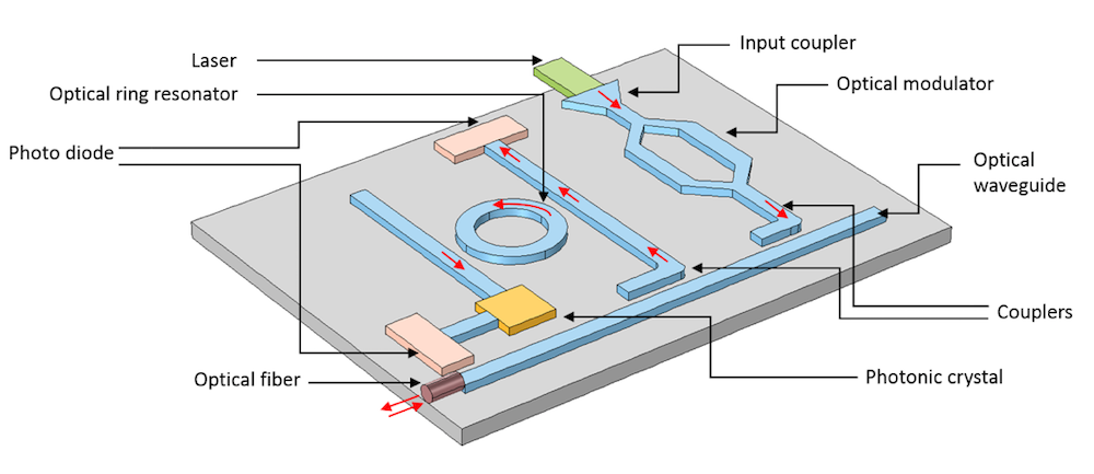
Figure 1: Cross-section of a silicon-on-insulator (SOI) waveguide showing light confinement in the crystalline silicon layer. The buried oxide provides optical isolation from the substrate.
By the mid-1990s, researchers had demonstrated basic silicon waveguides with acceptable losses. But silicon photonics still lacked the three critical active components needed for any useful system: light sources, modulators, and photodetectors.
Part II: The Breakthrough Decade (2000-2010)
2005: The Year Everything Changed
If there's a single year that defined silicon photonics, it's 2005. Two landmark papers published in Nature that year proved that silicon could do what many thought impossible.
Intel's Continuous-Wave Silicon Raman Laser
In February 2005, a team led by Haisheng Rong and Mario Paniccia at Intel published a paper that sent shockwaves through the photonics community: "A continuous-wave Raman silicon laser" [5]. They had built a laser—a continuous-wave laser—entirely in silicon.
The challenge was formidable. Silicon is an indirect bandgap semiconductor, meaning it doesn't emit light efficiently through electron-hole recombination like direct bandgap materials (GaAs, InP). But Rong's team exploited a different phenomenon: stimulated Raman scattering. When you pump silicon with intense laser light, the photons interact with silicon's crystal lattice vibrations (phonons), transferring energy and generating new photons at a longer wavelength.
The breakthrough was solving the two-photon absorption (TPA) problem. At high optical intensities, silicon absorbs two photons simultaneously, generating free carriers that absorb even more light—a vicious cycle that kills lasing. Rong's solution was elegant: embed a p-i-n diode structure directly into the waveguide. By reverse-biasing the diode, they swept out the free carriers as fast as TPA generated them.
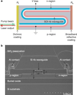
Figure 2: Intel's continuous-wave Raman laser waveguide structure (2005). The p-i-n diode (shown in cross-section) sweeps out free carriers generated by two-photon absorption, enabling continuous lasing. Source: Rong et al., Nature 2005 [5]
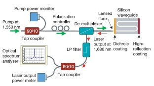
Figure 3: Experimental setup for the Intel Raman laser showing the pump laser, silicon waveguide, and detection system. Source: Rong et al., Nature 2005 [5]
The result: a silicon laser operating continuously at room temperature, producing milliwatts of optical power. As Paniccia later recalled, "few experts thought silicon could be used to build a laser" [3]. This paper has been cited over 1,672 times and remains one of the most influential in the field.
Michal Lipson's Micrometer-Scale Modulator
Just three months later, in May 2005, Michal Lipson and her team at Cornell published another Nature paper that would reshape the field: "Micrometre-scale silicon electro-optic modulator" [6]. They had built a modulator so small—just 12 micrometers in diameter—that it seemed to defy the laws of physics.
Traditional modulators were centimeters long. Lipson's was a microring resonator—a circular waveguide so small that light completes thousands of round trips in the time it takes to travel a millimeter. This creates a resonance effect: at specific wavelengths, light builds up inside the ring, amplifying any refractive index change by orders of magnitude.
By embedding electrodes in the ring and using the plasma dispersion effect, Lipson could shift the resonance wavelength by applying just a few volts. When the resonance aligned with the laser wavelength, light passed through. When it shifted away, light was blocked. The result: gigabit-per-second modulation in a device smaller than a human hair.
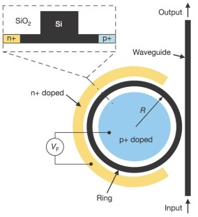
Figure 4: Schematic of Michal Lipson's microring resonator modulator (2005). The tiny 12-μm ring creates a resonance that amplifies the electro-optic effect, enabling ultra-compact, high-speed modulation. Source: Xu et al., Nature 2005 [6]
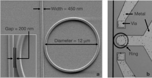
Figure 5: SEM and optical microscope images of the fabricated microring modulator showing the ring structure and coupling waveguide. Source: Xu et al., Nature 2005 [6]
In a 2021 interview, Lipson described the moment they first saw the device work: "I had goosebumps... It was one of those moments where you realize you've done something that will change the field." [7] The paper has been cited over 3,069 times—one of the most cited papers in all of photonics.
Lipson's philosophy on research is revealing: "Keep asking the 'why'. Don't just accept what people tell you. Creativity comes from questioning assumptions." [7] Her multicultural background—born in Brazil, educated in Israel, working in the USA—gave her a unique perspective that helped her see solutions others missed.
The Heterogeneous Integration Breakthrough
While Intel and Cornell were pushing the boundaries of silicon-only devices, John E. Bowers at UC Santa Barbara was pioneering a different approach: heterogeneous integration. Instead of forcing silicon to do everything, why not bond III-V semiconductor lasers (made from InP or GaAs) directly onto silicon chips?
In 2006, Bowers' group demonstrated the first electrically pumped hybrid silicon laser [8]. They grew an InP-based laser structure, flipped it upside down, and bonded it to a silicon waveguide using molecular bonding. The III-V material provided efficient light generation, while the silicon waveguide carried the light across the chip.
This "best of both worlds" approach has become the dominant method for integrating lasers with silicon photonics. By 2010, Bowers and Di Liang published a comprehensive review in Nature Photonics titled "Recent progress in lasers on silicon" [9], which has been cited over 1,341 times. The paper laid out the roadmap for heterogeneous integration that the industry still follows today.
Part III: From Components to Systems (2010-2020)
2014: Wavelength + Mode Multiplexing
As individual components matured, researchers began combining them into more complex systems. In 2014, Li-Wei Luo, working in Michal Lipson's lab at Cornell (now at Columbia), published a breakthrough paper in Nature Communications: "WDM-compatible mode-division multiplexing on a silicon chip" [10].
The paper demonstrated something remarkable: combining wavelength-division multiplexing (WDM)—where different colors of light carry different data streams—with mode-division multiplexing (MDM)—where different spatial modes of light in the same waveguide carry independent data. This multiplicative effect could increase data capacity by 10-100×.
The key innovation was a microring-based mode (de)multiplexer that could separate different spatial modes with low crosstalk while remaining compatible with WDM systems. The paper has been cited 964 times and opened the door to ultra-high-capacity optical interconnects.
2015: The First Photonic Microprocessor—A Watershed Moment
If the 2005 papers proved silicon photonics could work, the 2015 paper by Chen Sun, Vladimir Stojanović, and colleagues proved it could be transformative. Published in Nature in December 2015, the paper was titled "Single-chip microprocessor that communicates directly using light" [11]—and it delivered exactly what it promised.
This wasn't a test chip with a few optical devices. This was a complete, functional computer:
- 70 million transistors forming a dual-core RISC-V processor
- 850 photonic components (modulators, photodetectors, waveguides, couplers)
- 1 MB of SRAM memory
- All fabricated in a commercial 45nm CMOS-SOI process with zero changes to the foundry
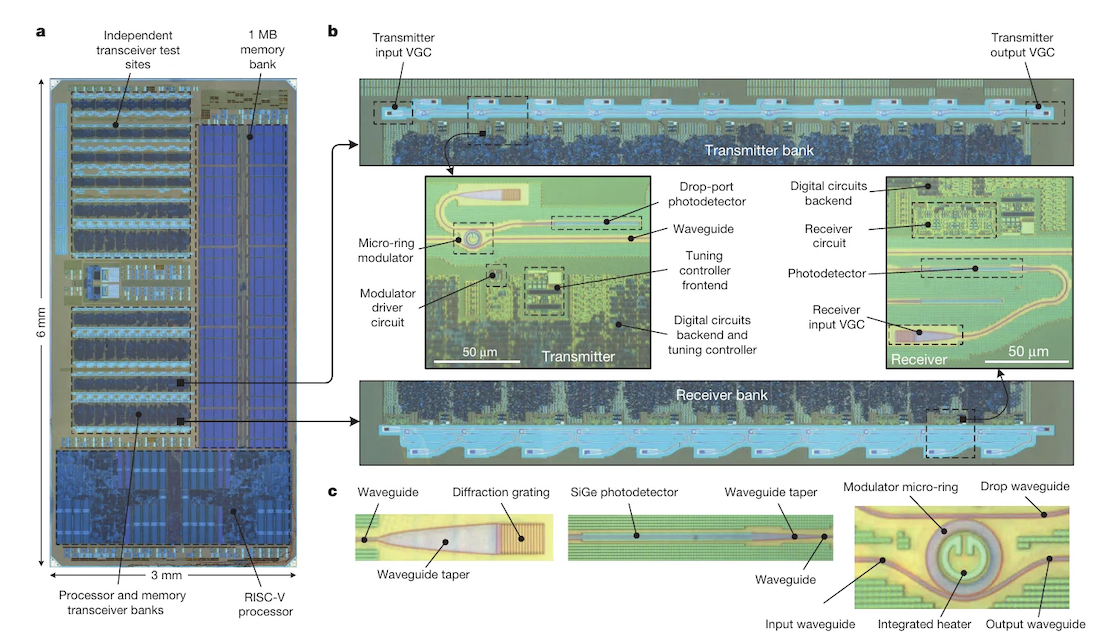
Figure 6: The first photonic microprocessor (2015). This 3mm × 6mm chip integrates a dual-core RISC-V processor, 1MB memory, and 850 photonic components, all fabricated in a standard CMOS process. Source: Sun et al., Nature 2015 [11]
The "zero-change" integration was crucial. Instead of requiring a custom fabrication process (which would be prohibitively expensive and incompatible with state-of-the-art electronics), the team designed all photonic devices to comply with the standard manufacturing rules of IBM's commercial process. This meant:
- Waveguides formed from the same crystalline silicon layer used for transistors
- Modulators using the same doping implants (n-well, p-well) used for transistors
The system demonstrated a processor optically communicating with remote memory over 20 meters of fiber at 2.5 Gb/s per direction (5 Gb/s aggregate). They ran real programs—including a 3D teapot rendering application and the STREAM memory benchmark—proving the system was fully functional.
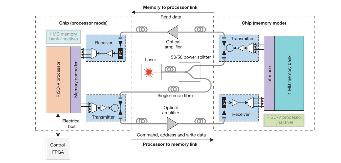
Figure 7: Block diagram of the photonic memory system. One chip acts as processor, the other as memory, connected by full-duplex optical links over 20m of fiber. Source: Sun et al., Nature 2015 [11]
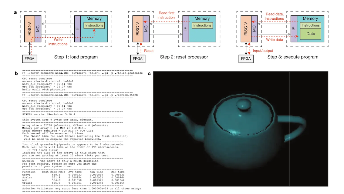
Figure 8: Demonstration of the photonic microprocessor running programs including "Hello World!" and a 3D teapot renderer, all communicating with memory over optical links. Source: Sun et al., Nature 2015 [11]
Perhaps most impressively, the team built thermal tuning control directly into the chip. Microring modulators are exquisitely sensitive to temperature—a few degrees can shift them out of resonance. The solution: integrate a microheater inside each ring, monitor the optical power with a photodetector, and use digital control circuits to lock the resonance to the laser wavelength. This feedback system compensated for temperature swings of 60 Kelvin and locked within 7 milliseconds at startup.
This paper represented a watershed moment. It proved that silicon photonics had matured from isolated components to complete systems-on-chip that could be manufactured in commercial foundries. The technology was ready for the real world.
2016: The Roadmap Paper
In 2016, a consortium of leading researchers including David Thomson, Andrew Zilkie, John E. Bowers, Tom Komljenovic, and many others published "Roadmap on silicon photonics" in the Journal of Optics [12]. This comprehensive review paper—cited over 1,553 times, making it one of the most cited papers in the field—laid out the state-of-the-art and future challenges across all areas of silicon photonics:
- Waveguide platforms and propagation loss reduction
- Optical sources: Raman lasers, heterogeneous integration, Ge lasers
- Modulators: ring resonators, Mach-Zehnder interferometers, plasma dispersion
- Photodetectors: Ge-on-Si, avalanche photodiodes, high-speed designs
- Integration approaches: monolithic vs. heterogeneous
- Packaging: fiber coupling, thermal management
- Applications: data centers, telecommunications, sensing, mid-IR
The roadmap provided a comprehensive snapshot of where the field stood after three decades of development and charted the path forward.
2018: MIT's Monolithic Integration
In 2018, Amir Atabaki, Sajjad Moazeni, and colleagues at MIT published another landmark paper in Nature: "Integrating photonics with silicon nanoelectronics for the next generation of systems on a chip" [13]. They demonstrated monolithic integration of photonics with 70 million transistors in a bulk CMOS process (not SOI).
The key innovation was fabricating photonic devices in polycrystalline silicon deposited on top of the CMOS electronics, rather than requiring the crystalline silicon layer of SOI wafers. This opened the door to integrating photonics with the vast majority of chips, which use bulk silicon substrates.
Figure 9: MIT's monolithic electronic-photonic integration platform (2018) showing photonics fabricated above CMOS electronics in a bulk silicon process. Source: Atabaki et al., Nature 2018 [13]
The paper has been cited over 1,015 times and demonstrated that silicon photonics could be integrated not just in specialized SOI processes, but in mainstream CMOS manufacturing.
Part IV: The AI Era and Beyond (2020-Present)
Lorenzo Pavesi's 30-Year Journey
In 2021, Lorenzo Pavesi of the University of Trento published a deeply personal reflection titled "Thirty years in silicon photonics: a personal view" [14]. Pavesi had been working on silicon photonics since the early 1990s, focusing on the quest for a silicon light source through quantum confinement in porous silicon and silicon nanocrystals.
His journey illustrates both the persistence required in this field and the evolution of its focus. While the dream of an efficient silicon LED or laser remains elusive, the field has thrived by embracing heterogeneous integration and finding applications where silicon's strengths—low cost, CMOS compatibility, dense integration—outweigh its weaknesses.
Pavesi's review traces the field's evolution through multiple application areas:
- Telecommunications (1990s-2000s): the original driver
- Optical interconnects (2000s-2010s): chip-to-chip and on-chip communication
- Sensing (2010s-present): biosensors, gas sensors, LiDAR
- Quantum photonics (2010s-present): quantum computing and communication
- Neuromorphic computing (2020s-present): optical neural networks for AI
2024: The Next-Generation Roadmap
In January 2024, a new generation of researchers published "Roadmapping the next generation of silicon photonics" in Nature Communications [15]. Led by Sudip Shekhar and including Wim Bogaerts (UGent-imec), Lukas Chrostowski (UBC), John E. Bowers (UCSB), Michael Hochberg, Richard Soref, and Bhavin J. Shastri, the paper introduced a generational framework analogous to Moore's Law:
| Generation | Acronym | Integration Scale | Characteristics | Era |
|---|---|---|---|---|
| Small-Scale Integration | SSI | <100 components | Discrete devices, basic transceivers | 1990s-2000s |
| Medium-Scale Integration | MSI | 100-1,000 components | WDM systems, coherent transceivers | 2000s-2010s |
| Large-Scale Integration | LSI | 1,000-10,000 components | Programmable circuits, optical switches | 2010s-2020s |
| Very Large-Scale Integration | VLSI | >10,000 components | Optical neural networks, quantum processors | 2020s-2030s |
The paper has already been cited 531 times in less than one year—a testament to its importance. It argues that silicon photonics is entering the VLSI era, where chips will contain tens of thousands of photonic components working in concert with billions of transistors.
The UGent-imec Photonics Research Group
One of the world's leading silicon photonics research centers is the Photonics Research Group at Ghent University (UGent) and imec in Belgium, led by Roel Baets and Wim Bogaerts [16]. The group has made seminal contributions to:
- Silicon photonics design tools: They developed open-source design kits and simulation tools used worldwide
- Programmable photonic circuits: Reconfigurable meshes of Mach-Zehnder interferometers that can be programmed for different functions
- Photonic integration platforms: Multi-project wafer (MPW) services that democratized access to silicon photonics fabrication
- Optical neural networks: Using programmable photonic circuits for AI acceleration
Bogaerts' work on programmable photonics has been particularly influential. Instead of designing fixed-function photonic circuits, his group builds reconfigurable meshes where each element can be tuned. This enables a single chip to perform multiple functions—wavelength routing, optical switching, signal processing—simply by changing the programming.
The UGent-imec group has trained generations of silicon photonics researchers and spun out multiple companies, making it a cornerstone of the European silicon photonics ecosystem.
The AI Revolution: Why Silicon Photonics Matters Now
The explosive growth of artificial intelligence has created an insatiable demand for computing power. Training large language models like GPT-4 requires moving vast amounts of data between processors, memory, and accelerators. Electrical interconnects are hitting fundamental limits:
- Bandwidth: Copper wires can't scale to the terabits-per-second needed
- Power: Moving data electrically consumes more power than the computation itself
- Latency: Electrical signals are limited by RC delays and signal integrity issues
Silicon photonics offers a solution. Optical interconnects can provide:
- Massive bandwidth: Wavelength-division multiplexing enables terabits/second on a single fiber
- Low power: Photons don't dissipate energy in wires like electrons do
- Low latency: Light travels at ~2/3 the speed of light in fiber, with minimal dispersion
Companies like Ayar Labs (founded by researchers from MIT, UC Berkeley, and Colorado), Lightmatter, and Celestial AI are building silicon photonic chiplets specifically for AI infrastructure. Ayar Labs has raised over $1 billion from investors including NVIDIA, Intel, AMD, and GlobalFoundries [17].
In October 2025, Sequoia Capital's endorsement of silicon photonics explicitly cited AI as the killer application: "The bottleneck in AI is multiplying big matrices, and you can do this efficiently with silicon photonics." [2]
Part V: The Technology Deep Dive
How Silicon Photonics Actually Works
At its core, silicon photonics exploits three key physical phenomena:
1. Total Internal Reflection and Waveguiding
Silicon has a refractive index of ~3.48 at 1.55 μm, while silicon dioxide (SiO₂) has an index of ~1.44. When light traveling in silicon hits the Si/SiO₂ interface at a shallow angle, it undergoes total internal reflection—bouncing back into the silicon rather than escaping.
By patterning silicon into narrow strips (typically 400-500 nm wide, 200-300 nm tall) surrounded by oxide, we create waveguides that confine light through total internal reflection on all sides. Light propagates along the waveguide with remarkably low loss—modern silicon waveguides achieve <1 dB/cm propagation loss.
2. Free-Carrier Plasma Dispersion Effect
The refractive index of silicon depends on the concentration of free carriers (electrons and holes). This is the plasma dispersion effect, first characterized by Soref and Bennett in 1987 [4]:
Δn = Δn_e(N_e) + Δn_h(N_h)
where Δn_e and Δn_h are the index changes due to electrons and holes, and N_e and N_h are their concentrations.
By embedding a p-n junction in a waveguide and applying a voltage, we can inject or deplete carriers, changing the refractive index. This enables:
- Modulators: Changing the index changes the optical phase, which can be converted to amplitude modulation using interferometers or resonators
- Switches: Routing light between different paths by changing waveguide indices
- Tunable filters: Shifting the resonance wavelength of ring resonators
3. Heterogeneous Integration and Bonding
Since silicon is an indirect bandgap semiconductor, it doesn't emit light efficiently. The solution: bond III-V semiconductors (InP, GaAs) that DO emit light efficiently directly onto silicon chips.
Molecular bonding (also called direct bonding or wafer bonding) works by:
- Preparing atomically smooth surfaces on both the III-V wafer and silicon wafer
- Bringing them into contact at room temperature—van der Waals forces hold them together
- Annealing at ~300°C to form permanent covalent bonds
The result: a hybrid structure where the III-V layer provides optical gain (lasing) while the silicon waveguide carries the light across the chip. This "best of both worlds" approach has become the industry standard for integrating lasers.
The Building Blocks: Key Components
Waveguides
- Strip waveguides: Rectangular silicon core, oxide cladding. Tight confinement, small bend radius (~5 μm), but polarization-dependent
- Rib waveguides: Silicon slab with raised ridge. Larger mode, lower loss, less polarization-dependent
- Slot waveguides: Narrow slot between two silicon rails. Concentrates light in the low-index slot for sensing applications
Modulators
- Microring modulators: Ultra-compact (5-20 μm diameter), low power (<1 mW), but temperature-sensitive and limited bandwidth (~50 GHz)
- Mach-Zehnder modulators: Two-arm interferometer, temperature-insensitive, high bandwidth (>100 GHz), but larger footprint (~1 mm)
- Traveling-wave modulators: Electrodes designed as transmission lines, enabling >100 GHz bandwidth
Photodetectors
- Ge-on-Si PIN photodetectors: Germanium epitaxially grown on silicon absorbs 1.3-1.55 μm light. Typical responsivity ~1 A/W, bandwidth >50 GHz
Couplers
- Grating couplers: Periodic structures that diffract light from waveguides into optical fibers. Typical efficiency ~50-75% (-1.2 to -3 dB)
- Edge couplers: Waveguides that taper to match fiber mode size. Higher efficiency (>90%) but require cleaved chip edges
Part VI: Risks and Opportunities
The Opportunities
1. AI and High-Performance Computing
The most immediate opportunity is optical interconnects for AI accelerators. As models grow to trillions of parameters, moving data between chips becomes the bottleneck. Silicon photonics can provide:
- Terabit/s bandwidth per fiber using dense WDM
- Picojoule/bit energy efficiency (100× better than electrical)
- Chip-to-chip, board-to-board, and rack-to-rack connectivity
2. Data Centers and Telecommunications
Silicon photonics is already deployed in data centers for 400G and 800G transceivers. The next frontier:
- 1.6 Tb/s and 3.2 Tb/s modules for AI clusters
- Co-packaged optics: Integrating photonics directly with switch ASICs
- Coherent transceivers: Using advanced modulation formats for long-haul transmission
3. LiDAR and Autonomous Vehicles
Solid-state LiDAR based on silicon photonics can provide:
- Optical phased arrays: Electronically steerable beams with no moving parts
- Frequency-modulated continuous wave (FMCW): Simultaneous range and velocity measurement
- CMOS-compatible manufacturing: Enabling $100 LiDAR sensors vs. $10,000 for mechanical systems
4. Quantum Computing and Communication
Silicon photonics is emerging as a platform for photonic quantum computing:
- Quantum entanglement generation: Using nonlinear processes in silicon waveguides
- Quantum gates: Programmable interferometers for quantum information processing
- Quantum communication: Integrated transmitters and receivers for quantum key distribution
5. Biosensing and Medical Diagnostics
Silicon photonic biosensors can detect:
- Single molecules: Using high-Q microring resonators
- Multiplexed biomarkers: Hundreds of sensors on a single chip
- Point-of-care diagnostics: CMOS-compatible manufacturing enables disposable sensors
The Risks
1. Thermal Sensitivity
Microring resonators shift ~10 pm/°C (picometers per degree Celsius). In a data center with varying workloads, this requires:
- Active thermal tuning: Heaters consume 1-10 mW per ring
- Athermal designs: Compensating structures that cancel temperature dependence
- Packaging: Thermal management to stabilize chip temperature
2. Manufacturing Yield and Variability
Silicon photonics requires nanometer-scale precision:
- Waveguide width variations of ±1 nm can shift resonances by 100 pm
- Thickness variations across wafers affect all devices
- Defects: Particles or process variations can kill entire chips
The solution: design for variability using robust device architectures and post-fabrication trimming using UV exposure or ion implantation to tune individual devices.
3. Packaging Costs
While silicon photonics chips are cheap to fabricate (leveraging CMOS fabs), packaging is expensive:
- Fiber attachment: Aligning fibers to grating couplers with sub-micron precision
- Laser integration: Bonding or flip-chip mounting III-V lasers
- Testing: Characterizing hundreds of optical ports per chip
Packaging can account for 50-80% of total module cost. The industry is developing:
- Automated fiber attachment using robotic pick-and-place
- Wafer-level testing to reduce test time
- Co-packaged optics to amortize packaging costs across multiple functions
4. Competing Technologies
Silicon photonics faces competition from:
- InP photonics: Mature technology with integrated lasers, but expensive and low volume
- Thin-film lithium niobate: Emerging platform with superior electro-optic effect
- Electrical interconnects: Continued improvements in copper and advanced signaling
The key question: Will silicon photonics' cost and integration advantages outweigh its material limitations?
Epilogue: The Road Ahead
As we stand in 2025, silicon photonics is at an inflection point. The technology has matured from laboratory curiosity to commercial reality. Millions of silicon photonic transceivers ship every year for data centers. Startups have raised billions to bring photonic AI accelerators to market. Venture capitalists who once dismissed the field as "too hard" are now calling it the next silicon revolution.
Yet fundamental challenges remain. We still don't have an efficient, electrically pumped silicon laser. Thermal tuning consumes power and adds complexity. Packaging costs limit deployment to high-value applications.
But if history has taught us anything, it's this: underestimate silicon photonics at your peril. Every decade, skeptics have declared it dead or impractical. Every decade, brilliant researchers have proven them wrong.
From Richard Soref's heretical idea in 1985, to Haisheng Rong's impossible laser in 2005, to Michal Lipson's goosebumps moment with the microring modulator, to Chen Sun's photonic microprocessor in 2015, to today's AI-driven renaissance—this field has been propelled by people who refused to accept "no" as an answer.
The next 50 years of silicon photonics may indeed mirror the last 50 years of silicon electronics. If so, we're only at the beginning of the journey.
"The best way to predict the future is to invent it." — Alan Kay
And in silicon photonics, the future is being invented right now.
References
[1] Soref, R. A. (1985). "Silicon-based optoelectronics." Proceedings of the IEEE, 81(12), 1687-1706. https://ieeexplore.ieee.org/document/468
[2] Sequoia Capital. (2025). "Seed and Venture Funds 2025." https://sequoiacap.com/article/seed-venture-funds-2025/
[3] SPIE Photonics Focus. (2025). "Pioneering Silicon Photonics: Richard Soref." https://spie.org/news/photonics-focus/marchapril-2025/pioneering-silicon-photonics
[4] Soref, R. A., & Bennett, B. R. (1987). "Electrooptical effects in silicon." IEEE Journal of Quantum Electronics, 23(1), 123-129. https://doi.org/10.1109/JQE.1987.1073206
[5] Rong, H., Jones, R., Liu, A., Cohen, O., Hak, D., Fang, A., & Paniccia, M. (2005). "A continuous-wave Raman silicon laser." Nature, 433(7027), 725-728. https://doi.org/10.1038/nature03346
[6] Xu, Q., Schmidt, B., Pradhan, S., & Lipson, M. (2005). "Micrometre-scale silicon electro-optic modulator." Nature, 435(7040), 325-327. https://doi.org/10.1038/nature03569
[7] SPIE Advanced Photonics. (2021). "Wonderland of silicon photonics—an interview with Professor Michal Lipson." https://www.spiedigitallibrary.org/journals/advanced-photonics/volume-3/issue-03/030501/
[8] Fang, A. W., Park, H., Cohen, O., Jones, R., Paniccia, M. J., & Bowers, J. E. (2006). "Electrically pumped hybrid AlGaInAs-silicon evanescent laser." Optics Express, 14(20), 9203-9210. https://doi.org/10.1364/OE.14.009203
[9] Liang, D., & Bowers, J. E. (2010). "Recent progress in lasers on silicon." Nature Photonics, 4(8), 511-517. https://doi.org/10.1038/nphoton.2010.167
[10] Luo, L. W., Ophir, N., Chen, C. P., Gabrielli, L. H., Poitras, C. B., Bergman, K., & Lipson, M. (2014). "WDM-compatible mode-division multiplexing on a silicon chip." Nature Communications, 5, 3069. https://doi.org/10.1038/ncomms4069
[11] Sun, C., Wade, M. T., Lee, Y., Orcutt, J. S., Alloatti, L., Georgas, M. S., ... & Stojanović, V. M. (2015). "Single-chip microprocessor that communicates directly using light." Nature, 528(7583), 534-538. https://doi.org/10.1038/nature16454
[12] Thomson, D., Zilkie, A., Bowers, J. E., Komljenovic, T., Reed, G. T., Vivien, L., ... & Nedeljkovic, M. (2016). "Roadmap on silicon photonics." Journal of Optics, 18(7), 073003. https://doi.org/10.1088/2040-8978/18/7/073003
[13] Atabaki, A. H., Moazeni, S., Pavanello, F., Gevorgyan, H., Notaros, J., Alloatti, L., ... & Popović, M. A. (2018). "Integrating photonics with silicon nanoelectronics for the next generation of systems on a chip." Nature, 556(7701), 349-354. https://doi.org/10.1038/s41586-018-0028-z
[14] Pavesi, L. (2021). "Thirty years in silicon photonics: a personal view." Frontiers in Physics, 9, 786028. https://doi.org/10.3389/fphy.2021.786028
[15] Shekhar, S., Bogaerts, W., Chrostowski, L., Bowers, J. E., Hochberg, M., Soref, R., & Shastri, B. J. (2024). "Roadmapping the next generation of silicon photonics." Nature Communications, 15, 751. https://doi.org/10.1038/s41467-024-44750-0
[16] Photonics Research Group, UGent-imec. https://www.photonics.intec.ugent.be/
[17] Ayar Labs. (2024). "Ayar Labs Announces $155M Series D Funding." https://ayarlabs.com/news/
Key Researchers Profiled
| Researcher | Institution | Key Contributions | Notable Papers |
|---|---|---|---|
| Richard A. Soref | Air Force Research Lab, UMass Boston | Founded the field (1985), plasma dispersion theory | Soref & Bennett (1987) - 10,000+ citations |
| Haisheng Rong | Intel | First CW silicon Raman laser (2005) | Rong et al., Nature (2005) - 1,672 citations |
| Mario Paniccia | Intel | Led Intel's silicon photonics program | Multiple Nature papers 2004-2010 |
| Michal Lipson | Cornell, Columbia, now Boston Univ | Microring modulator (2005), programmable photonics | Xu et al., Nature (2005) - 3,069 citations |
| John E. Bowers | UC Santa Barbara | Heterogeneous integration, hybrid lasers | Liang & Bowers (2010) - 1,341 citations |
| Roel Baets | UGent-imec | Silicon photonics platforms, design tools | Thomson et al. (2016) - 1,553 citations |
| Wim Bogaerts | UGent-imec | Programmable photonic circuits | Shekhar et al. (2024) - 531 citations |
| Yurii Vlasov | IBM | IBM Silicon Nanophotonics program | Multiple Nature papers 2008-2015 |
| Lorenzo Pavesi | University of Trento | Silicon light sources, quantum confinement | 30-year review (2021) |
| Vladimir Stojanović | MIT, UC Berkeley | Electronic-photonic integration, photonic processors | Sun et al., Nature (2015) |
| Chen Sun | UC Berkeley, MIT | First photonic microprocessor (2015) | Sun et al., Nature (2015) |