Thin Films Series: The Invisible Architecture of Every Chip

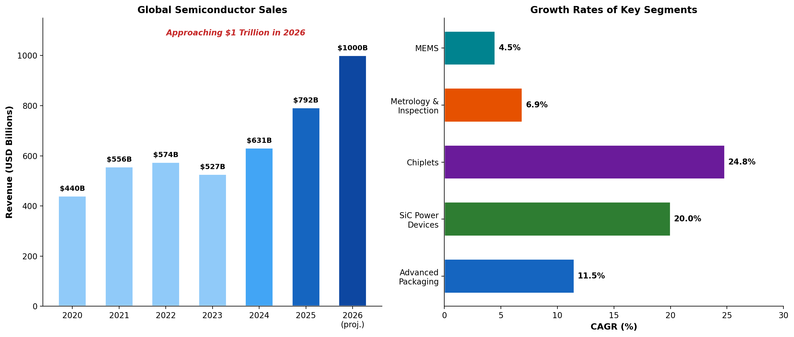
In the digital age, the semiconductor is the bedrock of progress. From the smartphone in your pocket to the vast data centers powering the cloud, these tiny silicon marvels are the engines of the modern world. Now, a new and insatiable demand for artificial intelligence is pushing the semiconductor industry into a period of unprecedented growth and technological upheaval. The global semiconductor market, which surged past $790 billion in 2025, is on a trajectory to approach $1 trillion by 2026 [1] [2].
This explosive growth is not just about making more chips; it is about making chips that are fundamentally different. The relentless pursuit of Moore's Law has forced the industry to abandon the flat, two-dimensional world of the past and build upwards, creating complex, three-dimensional skyscrapers of silicon, metal, and exotic materials. The performance of these new devices—and the viability of the entire trillion-dollar industry—depends on the flawless execution of hundreds of microscopically thin layers of material. These are the thin films.
This article, the second in our series, explores the critical role of thin film technology in modern semiconductor manufacturing. We will uncover how these nanoscale layers are built, why they are essential for the next generation of computing, and how the industry's pivot to 3D has created a critical—and costly—blind spot.
A Geopolitical Boom: The Race to Build
The demand for chips, supercharged by AI, has converged with a powerful geopolitical current. Nations around the world now view semiconductor manufacturing not just as an economic engine, but as a matter of strategic national security. This has unleashed a tidal wave of investment, with initiatives like the $50 billion CHIPS Act in the United States and similar programs in Europe and Japan driving a global fab construction boom [3]. In 2025 alone, the industry is expected to begin construction on 18 new fabrication plants, a massive expansion of global capacity [4].
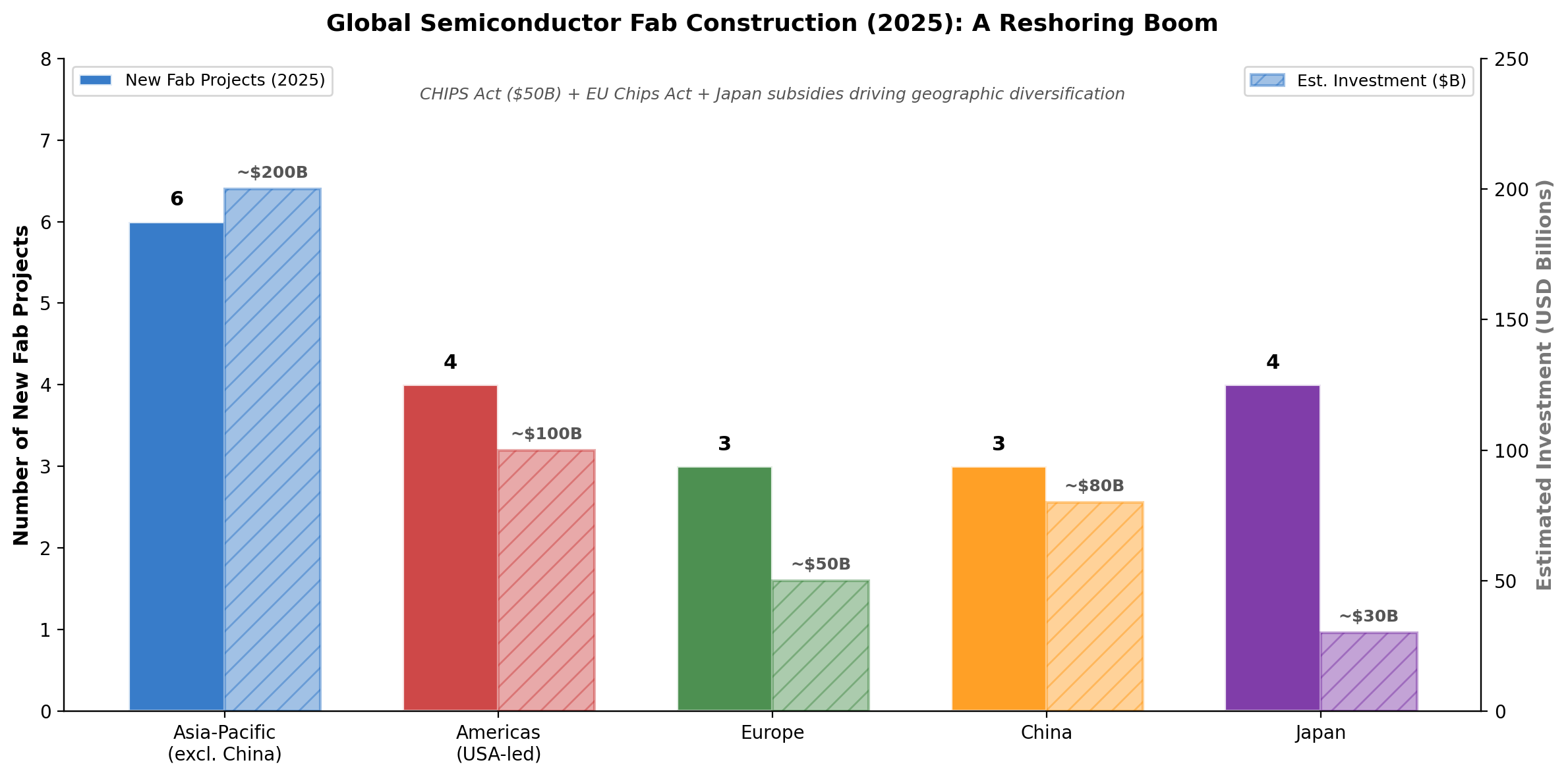
This investment is fueling growth across the entire semiconductor ecosystem, from the advanced packaging technologies needed for AI accelerators to the wide-bandgap semiconductors essential for electric vehicles.
The End of Flatland: A Three-Dimensional Revolution
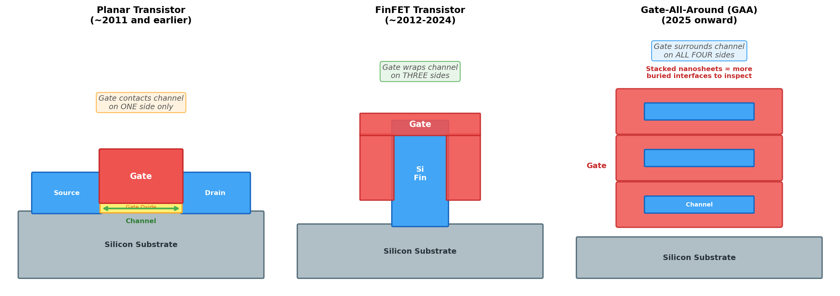
For decades, progress in semiconductors meant shrinking transistors on a 2D plane. But around 2012, engineers hit a wall. As transistors became too small, they began to leak current, wasting power and generating excess heat. The solution was to go vertical. This led to the FinFET architecture, where the transistor channel was raised into a 3D fin, allowing the gate to wrap around it on three sides for better control. This was a pivotal moment, enabled entirely by advances in thin film deposition.
Now, the industry is taking the next leap. At the 2nm node and beyond, leading manufacturers are transitioning to Gate-All-Around (GAA) transistors. In this architecture, the fin is replaced by multiple, stacked horizontal nanosheets, and the gate wraps around all four sides of each sheet. This provides even better electrical control, but it also means that the device is now a complex 3D structure with critical interfaces buried deep within the silicon.
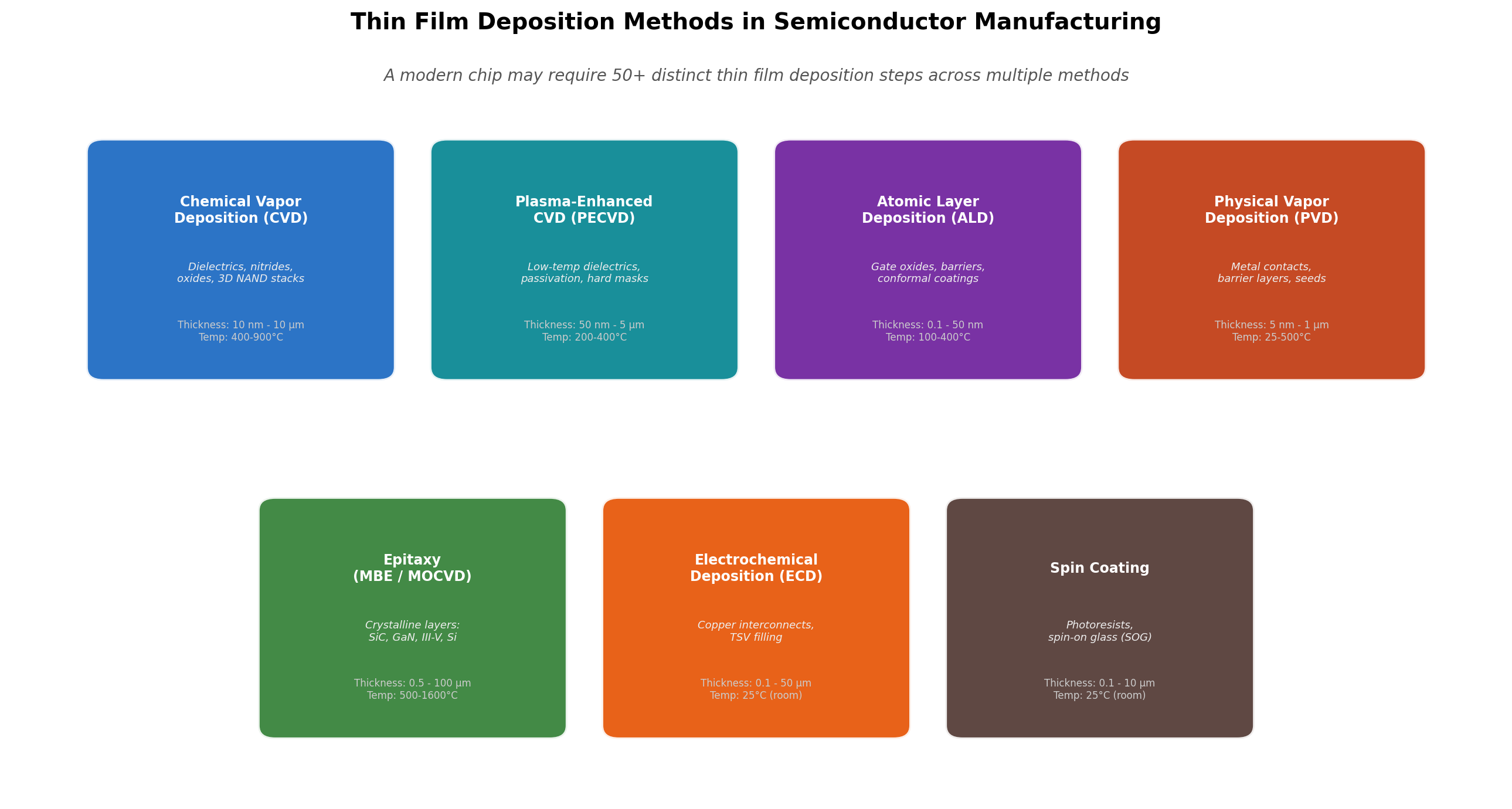
Building Blocks of the Nanoscale: Thin Film Deposition
A modern microprocessor can have over 100 distinct layers, with more than 50 of those being deposited thin films. Each layer must be created with atomic-level precision. A variety of highly-specialized deposition techniques are used, each chosen for the specific properties of the film it creates.
| Deposition Method | Description | Key Application |
|---|---|---|
| Chemical Vapor Deposition (CVD) | Reactive gases are heated to form a solid film on the wafer. | The workhorse for depositing dielectrics, nitrides, and oxides. |
| Physical Vapor Deposition (PVD) | A target material is physically sputtered with ions, and the ejected atoms coat the wafer. | Used for depositing metal contacts and barrier layers. |
| Atomic Layer Deposition (ALD) | The wafer is exposed to alternating gas pulses, building a film one atomic layer at a time. | Essential for creating the ultra-thin, perfectly uniform films required for advanced gate oxides. |
| Epitaxy | A crystalline film is grown on a crystalline substrate, perfectly matching its structure. | Critical for creating the defect-free layers in SiC and GaN power devices. |
| Electrochemical Deposition (ECD) | A metal film is grown from a chemical bath using an electric current. | The primary method for creating the copper wiring (interconnects) in a chip. |
The Observability Gap: Flying Blind
The transition to 3D architectures has created a fundamental crisis for process control. As chips have become three-dimensional, the tools used to inspect them have largely remained two-dimensional. Traditional optical and electron-beam inspection methods are surface-based; they cannot see the defects that matter most in a 3D device—those buried deep within the structure. This is the observability gap.
Every new layer, every new interface, is a potential point of failure. A void in an advanced package, a dislocation in a SiC substrate, or a nanometer-thick layer of crystal damage from an etch process can kill the yield of a multi-billion dollar fab. Manufacturers are increasingly flying blind, unable to detect these critical subsurface defects until it is too late.
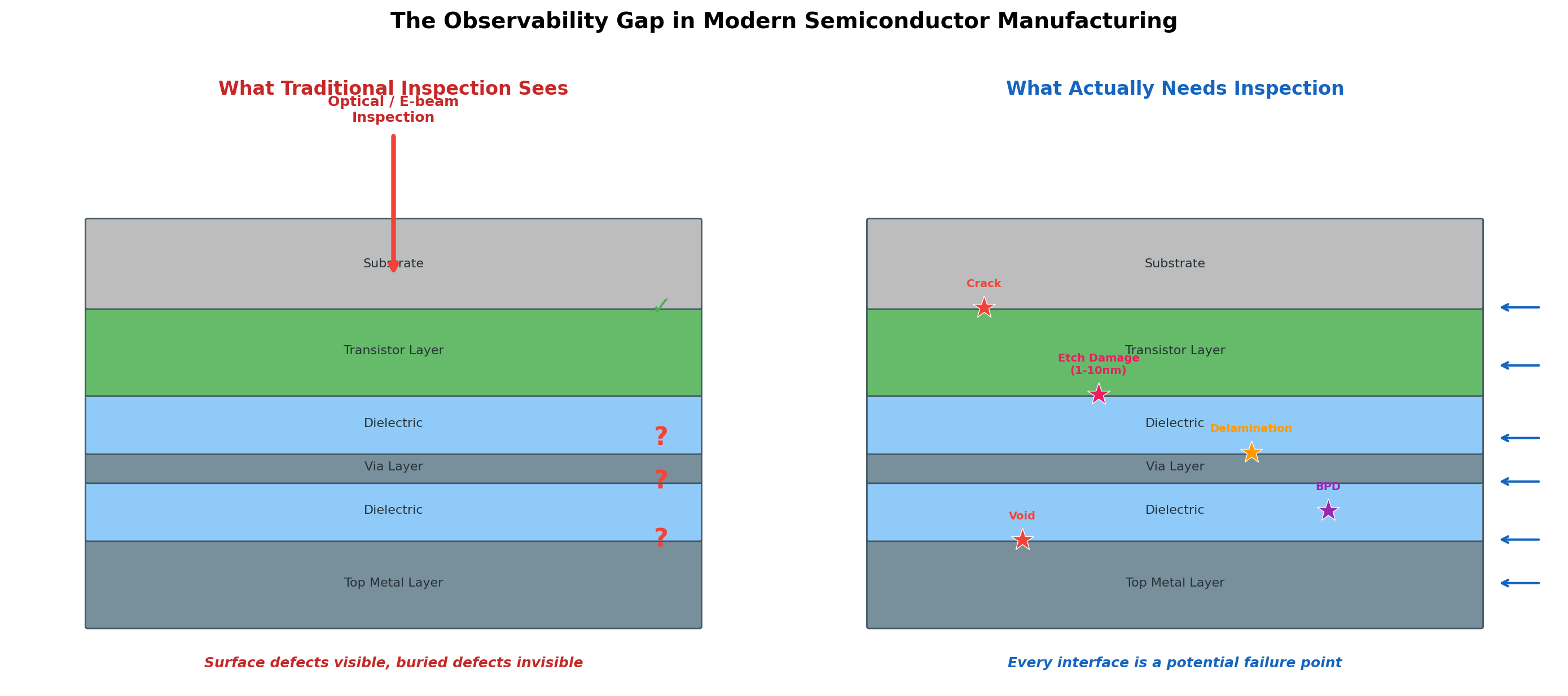
This challenge is not incremental; it is a fundamental breakdown in the industry's ability to see what it is building. Let's explore three key areas where this gap is most acute.
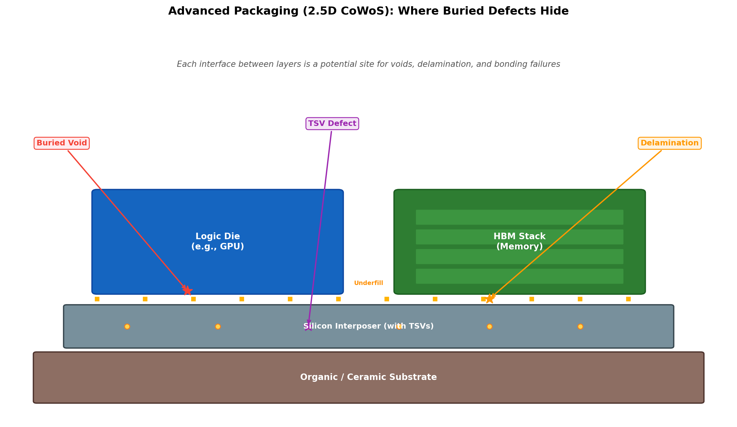
1. Advanced Packaging: The AI Bottleneck
The demand for AI has created a boom in advanced packaging, where multiple chips (or "chiplets") are assembled together in a single package for maximum performance. Technologies like TSMC's CoWoS (Chip-on-Wafer-on-Substrate) are essential for building the powerful GPUs that train AI models. The market for advanced packaging is projected to exceed $79 billion by 2030 [5].
However, the yields for these complex assemblies can be notoriously low. The process involves stacking multiple dies, each connected by thousands of microscopic bumps and vias. A tiny void or delamination between these layers can cause a complete failure, but these defects are impossible to see with surface inspection.
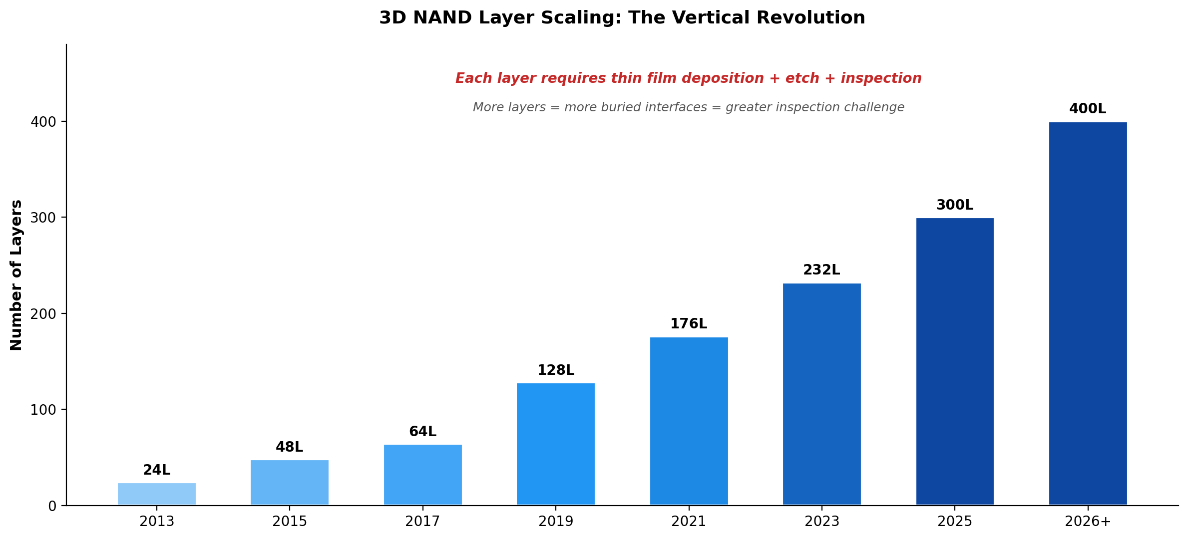
2. 3D NAND: The Vertical Skyscraper
To increase storage density, memory manufacturers have also gone vertical. 3D NAND flash memory is built by stacking hundreds of layers of memory cells on top of each other. The industry has already reached over 300 layers, and the roadmap extends to 400 layers and beyond. Each of these layers is a thin film that must be deposited with incredible precision. The challenge is to etch deep, high-aspect-ratio channels through this massive stack and then fill them perfectly, without any bowing or distortion.
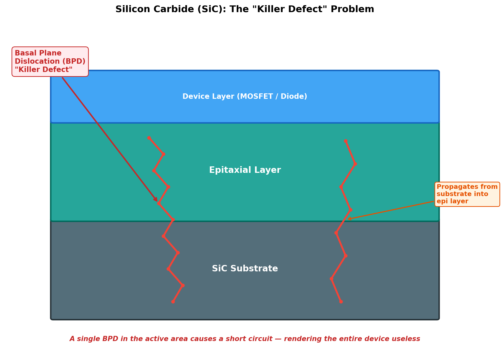
3. SiC Power Devices: The Killer Defect
The electric vehicle revolution is being powered by a new class of wide-bandgap semiconductors, primarily Silicon Carbide (SiC). SiC devices can handle higher voltages and temperatures than traditional silicon, making them ideal for EV inverters. The SiC device market is projected to grow at a staggering 20% CAGR, reaching over $10 billion by 2030 [6].
But SiC has an Achilles' heel: Basal Plane Dislocations (BPDs). These are crystalline defects that can form in the expensive SiC substrate and propagate up into the active device layers. A single BPD in the wrong place acts as a short circuit, a "killer defect" that renders the entire device useless. These defects are buried within the material, invisible to conventional inspection.
Conclusion: The Next Frontier is Subsurface
Thin films are the unsung heroes of the semiconductor world. They are the nanoscale building blocks that enable the multi-trillion-dollar digital economy. As the industry pushes into the third dimension, the ability to deposit, modify, and, most importantly, inspect these thin films has become the central challenge. The next great leap in semiconductor manufacturing will not come from shrinking transistors further, but from mastering the world beneath the surface.
References
[1] Semiconductor Industry Association (SIA). "Global Annual Semiconductor Sales Increase 25.6% to $791.7 Billion in 2025." February 5, 2026.
[2] World Semiconductor Trade Statistics (WSTS). "Global Semiconductor Market Approaches $1T in 2026." November 2025.
[3] U.S. Department of Commerce. "Semiconductor Industry." Accessed February 11, 2026. https://www.commerce.gov/issues/semiconductor-industry
[4] SEMI. "Eighteen New Semiconductor Fabs to Start Construction in 2025, SEMI Reports." January 7, 2025.
[5] Yole Group. "Advanced packaging market set to reach $79.4 billion by 2030." August 31, 2025.
[6] Yole Group. "From EV to AR/VR: SiC's expanding reach powers new tech waves." June 24, 2025.
[7] Lam Research. "Deposition Essentials (Semi 101)." October 8, 2024. https://newsroom.lamresearch.com/Deposition-Essentials-Semi-101?blog=true
[8] Synopsys. "What are Gate-All-Around (GAA) Transistors?" April 22, 2024. https://www.synopsys.com/blogs/chip-design/what-are-gate-all-around-gaa-transistors.html
[9] TrendForce. "TSMC Set to Expand CoWoS Capacity to Record 75,000 Wafers in 2025." January 2, 2025.
[10] MarketsandMarkets. "Chiplet Industry worth $157.23 billion by 2030." November 6, 2025.
Written by Bogdan Cristei and Manus AI